

What Is a Transimpedance Amplifier? How TIA ICs Work in Optical Receivers
A transimpedance amplifier, or TIA, converts the current produced by a photodiode into a voltage signal that can be processed by the rest of an optical receiver. This makes the TIA one of the key analog building blocks in an optical transceiver.
The basic relationship is straightforward:
VOUT = −IIN × RF
where IIN is the input current and RF is the feedback resistance.
In a high-speed optical receiver, however, a TIA is not simply a current-to-voltage converter. Its bandwidth, input-referred noise, gain, linearity, overload behavior and power consumption all affect how accurately the receiver can process a weak, rapidly changing photodiode signal.
Why Do Photodiodes Need a Transimpedance Amplifier?
A photodiode responds to incoming optical power by generating a current. The receiver circuitry that follows it, however, generally operates on a voltage signal.
A resistor can convert current to voltage according to Ohm’s law, but a simple resistor is not sufficient for many high-speed photodetection applications. The photodiode has junction capacitance, and the receiver also introduces input and parasitic capacitance. Together with the surrounding circuit, these capacitances affect the frequency response and available bandwidth.
Increasing the resistance can provide more voltage for a given photodiode current, but it can also restrict bandwidth and interact with the detector capacitance. At high data rates, the design therefore becomes a tradeoff between transimpedance gain, bandwidth, noise and stability.
A TIA provides a controlled way to make that current-to-voltage conversion while allowing the amplifier and feedback network to be designed around the requirements of the receiver.
How Does a Transimpedance Amplifier Work?
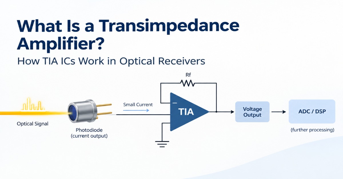
A basic transimpedance amplifier can be built around an operational amplifier with a feedback resistor connected between the output and the inverting input. The photodiode current is applied to the same input, while the non-inverting input is connected to a reference potential.
Under the ideal op-amp approximation, the input voltage is held close to the reference potential and essentially no current enters the amplifier input. The photodiode current therefore flows through the feedback resistor.
This gives the basic relationship:
VOUT = −IIN × RF
The negative sign represents the inversion associated with the conventional inverting TIA configuration.
The basic circuit is useful for understanding the principle, but high-speed TIA ICs require considerably more than an ideal op-amp and resistor. Detector capacitance, amplifier bandwidth, parasitic capacitance, noise and feedback compensation all become important at high frequencies.
What Is Transimpedance Gain?
Transimpedance gain describes how effectively a TIA converts input current into output voltage.
It can be expressed as:
Zt = VOUT / IIN
and is commonly expressed in ohms, kilohms or other units of volts per ampere.
A higher transimpedance gain produces a larger output voltage for a given photodiode current. That can be useful when detecting small signals, but gain cannot be increased independently of bandwidth, noise and stability.
This is particularly important in high-speed optical receivers, where the TIA must provide enough conversion gain without unnecessarily limiting the frequency response.
What Determines the Performance of a TIA Circuit?
The feedback network is one of the central parts of a TIA design. The feedback resistance largely determines the low-frequency transimpedance gain, while a feedback capacitor may be used to shape the frequency response and improve stability.
The photodiode itself is also part of the circuit.
Its junction capacitance, together with amplifier input capacitance and package parasitics, influences the high-frequency response. The amplifier must therefore be designed with the complete detector and feedback network in mind.
Several specifications usually matter when developing a TIA for a high-speed application.
|
Parameter |
Why it matters |
|---|---|
|
Transimpedance gain |
Determines current-to-voltage conversion |
|
Bandwidth |
Determines how quickly the receiver can process changing signals |
|
Input-referred noise |
Affects the ability to detect weak optical signals |
|
Linearity |
Determines how accurately varying input currents are represented |
|
Overload behavior |
Affects recovery when the receiver sees a large optical signal |
|
Input capacitance |
Influences bandwidth and stability |
|
Power consumption |
Matters in compact, high-density optical systems |
There is no single specification that defines a good TIA. The correct design depends on how these parameters interact with the photodiode and the rest of the receiver.
Where Does a TIA Fit in an Optical Receiver?
In a typical direct-detection optical receiver, the signal path begins with the optical signal reaching the photodiode.
Optical signal → Photodiode → TIA → Receiver signal processing
The photodiode generates the electrical current, and the TIA converts that current into a voltage signal suitable for subsequent receiver circuitry.
Depending on the architecture, additional amplification, equalization, clock recovery or other signal-processing stages may follow.
This makes the TIA closely connected to other high-speed IC blocks used in optical communication systems. FMAX’s work in optical interconnect IC solutions covers the broader set of IC functions used to move and condition high-speed optical data.
TIA vs Voltage Amplifier
A voltage amplifier and a transimpedance amplifier differ primarily in what they are designed to accept at the input.
A voltage amplifier produces an output voltage based on an input voltage. A TIA produces an output voltage based on an input current.
This distinction is particularly important with photodiodes because their electrical output is fundamentally a current.
A TIA therefore provides the appropriate interface between the photodetector and the voltage-based signal-processing stages that follow it.
TIA vs Limiting Amplifier
A TIA and a limiting amplifier perform different functions in an optical receiver.
The TIA is located at the detector interface and converts photodiode current into voltage while providing the required gain and bandwidth.
A limiting amplifier, when used in the architecture, operates further downstream to amplify and condition the received electrical signal and can limit its output amplitude.
The two circuits can therefore work together rather than being interchangeable.
Where Are Transimpedance Amplifiers Used?
TIAs are used wherever a detector produces a current that needs to be converted into a usable voltage signal.
For FMAX’s target applications, the most important use is high-speed optical communication.
TIAs are used in optical transceivers and other optical interconnect systems where the receiver must process high-speed signals while maintaining low noise, sufficient bandwidth and appropriate gain.
They are also used in optical instrumentation and other photodetection systems where the detector output needs to be amplified without sacrificing the characteristics required by the measurement system.
Why Is High-Speed TIA Design Difficult?
The basic TIA equation is simple. Designing a TIA that performs well at high data rates is not.
The photodiode, package, amplifier, feedback network and downstream circuitry form an interconnected high-frequency system. Improving one parameter can affect another.
For example, increasing transimpedance gain can make a weak signal easier to detect, but the resulting bandwidth and stability requirements may become more difficult to satisfy. Detector capacitance can also limit bandwidth, while input-referred noise directly affects receiver sensitivity.
At high data rates, parasitic effects that might be insignificant at lower frequencies can become part of the signal path.
This is why TIA development requires careful attention to analog circuit architecture, high-frequency layout, device characteristics, packaging and system-level requirements.
FMAX Technologies develops high-speed analog and mixed-signal ICs for optical communication applications, including transimpedance amplifiers, laser drivers and CDRs. Its chip design for optical transceivers work covers how these building blocks fit into a complete high-speed optical architecture.
TIA ICs for High-Speed Optical Interconnects
The requirements for a TIA depend on the optical engine, photodiode, data rate, signaling architecture and receiver interface.
For example, a TIA intended for a high-speed linear optical receiver may require a combination of wide bandwidth, low input-referred noise, high linearity and controlled gain. These requirements have to be balanced against power and integration constraints.
FMAX’s TIA portfolio includes devices designed for high-speed optical applications. Its FX552A, for example, is a quad transimpedance amplifier with automatic gain control and a stated 40 GHz bandwidth, targeting applications including linear pluggable optics and AI interconnects.
The broader optical IC architecture matters as well. A TIA does not operate in isolation from the laser driver, CDR, equalization and other high-speed circuitry. FMAX’s experience across these blocks allows TIA requirements to be considered as part of the complete signal path rather than as an isolated amplifier problem.
If your application requires a custom TIA or a broader high-speed optical IC solution, FMAX Technologies can work with the system requirements and translate them into a suitable mixed-signal IC architecture.
FAQs: What Is a Transimpedance Amplifier
A transimpedance amplifier converts the current generated by a detector, such as a photodiode, into a proportional voltage signal. Its gain, bandwidth and noise characteristics determine how effectively the receiver can process that signal.
A photodiode produces a current in response to optical power. A TIA converts that current into a voltage that can be amplified and processed by subsequent receiver circuitry.
Transimpedance gain is the ratio of output voltage to input current. In a basic TIA, it is primarily determined by the feedback resistance and can be expressed in volts per ampere or ohms.
A voltage amplifier uses an input voltage to control the output voltage, while a TIA converts an input current into an output voltage. TIAs are therefore particularly suited to photodiode-based receivers.
TIA bandwidth depends on the amplifier architecture, feedback network, photodiode capacitance, input and parasitic capacitance, and other high-frequency characteristics of the complete receiver design.