
Common Causes of Jitter in High-Speed Communication Systems
As data rates continue to increase across data centers, AI infrastructure, optical networks, and high-performance computing (HPC), maintaining signal integrity has become one of the biggest engineering challenges. Among the factors that degrade link performance, jitter is one of the most critical because it directly affects timing accuracy, eye opening, and bit error rate (BER).
Whether you’re designing a 100G Ethernet interface or an 800G optical transceiver, understanding the causes of jitter is essential for building reliable high-speed communication systems.
What Is Jitter in High-Speed Communication Systems?
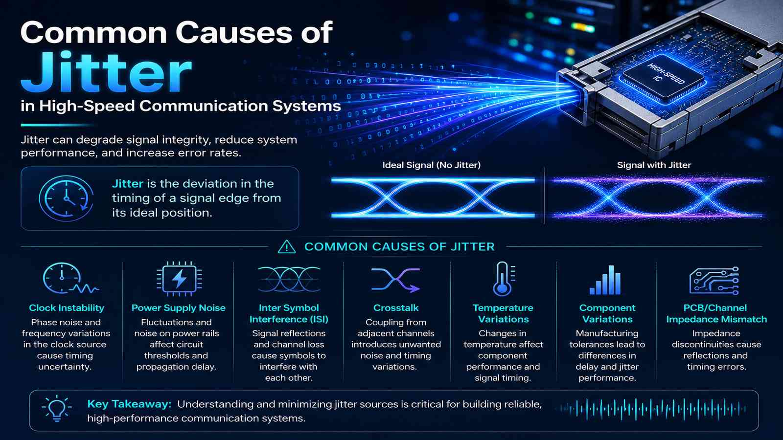
Jitter is the variation in the timing of a digital signal’s transitions from their ideal positions. Instead of switching exactly when expected, signal edges arrive slightly earlier or later, reducing the receiver’s ability to distinguish valid data.
As communication speeds increase, even picoseconds of timing variation can significantly impact system performance.
If jitter exceeds the receiver’s timing margin, the result can include:
-
Increased bit error rate (BER)
-
Eye diagram closure
-
Clock recovery failures
-
Data corruption
-
Reduced communication reliability
For high-speed interfaces, controlling jitter is just as important as maintaining voltage integrity.
Why Jitter Becomes More Critical at Higher Data Rates
As serial links move from 25 Gbps to 56 Gbps, 112 Gbps, and beyond, each transmitted bit occupies less time.
For example:
-
At 25 Gbps, each bit lasts approximately 40 picoseconds.
-
At 112 Gbps, each bit lasts less than 9 picoseconds.
With such narrow timing windows, small variations that were once insignificant can consume a large portion of the available eye opening, making systems far more susceptible to timing errors.
Random Jitter
Random jitter (RJ) is caused by unpredictable physical phenomena that cannot be completely eliminated.
Common sources include:
-
Thermal noise
-
Semiconductor device noise
-
Shot noise
-
Power supply fluctuations
-
Oscillator phase noise
Random jitter follows a statistical distribution and accumulates over time, making it difficult to predict individual timing deviations.
Although designers cannot eliminate random jitter entirely, selecting low-noise clock sources and optimizing analog circuitry helps reduce its impact.
Deterministic Jitter
Unlike random jitter, deterministic jitter (DJ) originates from identifiable system behaviors and is often repeatable.
Typical causes include:
-
Impedance discontinuities
-
PCB reflections
-
Crosstalk
-
Duty cycle distortion
-
Poor transmitter equalization
-
Connector discontinuities
Because deterministic jitter has identifiable causes, engineers can often reduce it through better channel design and careful layout practices.
Inter-Symbol Interference (ISI)
Inter-Symbol Interference occurs when previous transmitted symbols influence the current symbol due to channel bandwidth limitations.
Long PCB traces, connectors, cables, and vias introduce frequency-dependent losses that distort signal edges.
As a result:
-
Rising edges slow down.
-
Falling edges become distorted.
-
Eye openings shrink.
-
Timing uncertainty increases.
ISI becomes increasingly severe in multi-gigabit communication systems and is one of the primary reasons advanced equalization techniques are required.
Clock Jitter
The system clock provides the timing reference for both transmission and data recovery.
If the clock itself contains excessive phase noise or instability, every downstream component inherits that timing uncertainty.
Clock jitter commonly originates from:
-
Low-quality oscillators
-
PLL instability
-
Reference clock noise
-
PCB power noise
-
Poor clock distribution networks
Maintaining a clean reference clock is fundamental to achieving reliable high-speed communication.
Power Supply Noise
Power integrity directly influences timing performance.
Voltage fluctuations alter transistor switching characteristics, introducing variations in propagation delay across high-speed circuits.
Power supply noise may result from:
-
Inadequate decoupling
-
Switching regulators
-
Shared power planes
-
Simultaneous switching outputs (SSO)
-
Poor grounding
Effective power distribution network (PDN) design helps minimize these timing variations.
Crosstalk Between High-Speed Channels
As PCB routing density increases, neighboring signal traces begin interacting electromagnetically.
Aggressive routing can introduce:
-
Near-end crosstalk (NEXT)
-
Far-end crosstalk (FEXT)
These unwanted coupled signals distort transition timing and reduce overall signal integrity.
Proper spacing, differential routing, reference plane continuity, and controlled impedance help reduce crosstalk-induced jitter.
Impedance Mismatch and Signal Reflections
Every discontinuity along the signal path reflects a portion of the transmitted waveform.
Common reflection sources include:
-
Connectors
-
Vias
-
Packages
-
PCB layer transitions
-
Poor impedance control
Reflected energy overlaps with subsequent data transitions, increasing timing uncertainty and degrading receiver performance.
Maintaining consistent characteristic impedance throughout the communication channel minimizes reflections and associated jitter.
Electromagnetic Interference (EMI)
External electromagnetic fields can interfere with high-speed signals, introducing additional timing errors.
Potential EMI sources include:
-
High-current power circuits
-
Switching power supplies
-
Wireless transmitters
-
Electric motors
-
Adjacent digital systems
Good PCB layout practices, shielding, grounding, and differential signaling help improve immunity to external interference.
Temperature Variations
Temperature affects semiconductor switching speed, propagation delay, and oscillator stability.
In environments with significant thermal variation, timing characteristics may shift enough to increase overall jitter.
Thermal management strategies-including adequate cooling, optimized airflow, and careful component placement-help maintain stable performance.
How Engineers Reduce Jitter in High-Speed Systems
Managing jitter requires optimization across the entire communication channel rather than focusing on a single component.
Common techniques include:
-
Using low-phase-noise reference clocks
-
Maintaining controlled impedance PCB routing
-
Minimizing via discontinuities
-
Applying transmitter and receiver equalization
-
Optimizing power distribution networks
-
Reducing crosstalk through proper trace spacing
-
Implementing high-quality Clock and Data Recovery (CDR)
-
Selecting high-performance analog front-end circuits
-
Performing comprehensive channel simulation before fabrication
Successful designs treat jitter management as a system-level challenge rather than an isolated hardware issue.
The Role of High-Speed IC Design in Jitter Performance
High-speed integrated circuits play a central role in minimizing timing uncertainty.
Critical building blocks include:
-
Clock and Data Recovery (CDR) ICs
-
Laser Driver ICs
-
Transimpedance Amplifiers (TIAs)
-
High-speed Redriver ICs
-
Precision timing circuits
-
Mixed-signal analog front ends
Each device must preserve signal quality while minimizing additional jitter introduced into the communication channel.
FMAX Technologies develops high-speed analog and mixed-signal IC solutions for optical networking, instrumentation, and advanced communication systems. Through expertise in Clock and Data Recovery (CDR) ICs, Laser Driver ICs, Transimpedance Amplifiers (TIAs), Copper Redriver ICs, and custom mixed-signal IC development, FMAX helps equipment manufacturers improve signal integrity in demanding high-bandwidth applications.
FAQs: Causes of Jitter in High-Speed Communication Systems
There is no single cause. Jitter is typically the result of multiple factors, including channel loss, clock instability, power supply noise, crosstalk, impedance mismatches, and thermal effects.
No. Random jitter is an inherent characteristic of electronic systems. However, careful IC design, PCB layout, clock architecture, and signal conditioning can significantly reduce total jitter.
PAM4 uses four voltage levels, creating smaller eye openings than NRZ signaling. This makes PAM4 receivers more sensitive to timing variations, requiring advanced equalization, Forward Error Correction (FEC), and precise Clock and Data Recovery (CDR).
A Clock and Data Recovery (CDR) IC extracts a clean timing reference from incoming data, filters timing variations, and retimes the signal to improve communication reliability in high-speed serial links.